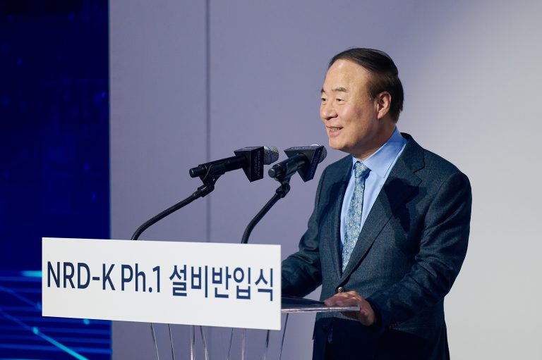
Samsung Electronics Co., Ltd. has announced the completion of a significant milestone in the development of its cutting-edge semiconductor research and development complex, NRD-K, located at the company’s Giheung campus. This achievement was marked by a tool-in ceremony attended by 100 guests, including prominent suppliers and customers, who gathered to celebrate the opening of the state-of-the-art facility.
State-of-the-Art Research Hub for Future Technologies
The NRD-K complex, which broke ground in 2022, is poised to become a pivotal research base for Samsung’s semiconductor innovations. The facility will focus on key areas including memory semiconductors, system LSI, and foundry technologies, providing a unified space for research and product-level verification. This advanced infrastructure will enable Samsung to further accelerate the pace of its technological advancements.
The company plans to invest approximately KRW 20 trillion by 2030 into the complex, which will span 109,000 square meters at the Giheung campus. A dedicated R&D production line is set to begin operations by mid-2025, further solidifying the facility’s role in Samsung’s long-term semiconductor strategy.
A Legacy of Innovation Continues in Giheung
In his remarks at the ceremony, Young Hyun Jun, Vice Chairman and Head of Samsung’s Device Solutions Division, stated, “The NRD-K complex will greatly enhance our ability to innovate, creating a seamless cycle of research, development, and mass production. This investment is not just about advancing our technology, but also about honouring our 50-year legacy in the semiconductor industry, as Giheung remains at the heart of our pioneering efforts.”
Samsung’s Giheung campus has a rich history of semiconductor innovation, famously marking the birthplace of the world’s first 64-megabit DRAM in 1992. The new NRD-K complex will continue this legacy by enabling next-generation developments in memory semiconductors, including 3D DRAM and V-NAND technologies, pushing the boundaries of memory storage with more than 1,000 layers.
Strategic Collaborations Drive Future Growth
Samsung’s push for next-gen innovations is further supported by its partnerships with key industry leaders. Park Gwang-Sun, Head of Applied Materials Korea, remarked, “In an era where collaboration is crucial for advancing technology, Applied Materials is committed to accelerating innovation alongside Samsung. By working together, we aim to drive the semiconductor industry forward and create a new wave of growth.”
The NRD-K complex will feature advanced equipment, including High NA extreme ultraviolet (EUV) lithography, and innovative material deposition technologies. Additionally, the facility will include infrastructure for wafer bonding, with cutting-edge wafer-to-wafer bonding capabilities designed to enhance manufacturing processes.
Commitment to Leading Semiconductor Advancements
In the third quarter of this year, Samsung invested a record KRW 8.87 trillion in R&D, underscoring the company’s continued focus on advancing semiconductor technologies. Through this investment, Samsung aims to strengthen its leadership position in the industry, particularly in advanced packaging for high-bandwidth memory (HBM) production, ensuring its competitive edge for years to come.
Samsung’s NRD-K complex marks a crucial step in the company’s long-term vision for the semiconductor industry. By integrating research, development, and manufacturing into one advanced facility, Samsung is reinforcing its commitment to shaping the future of memory and semiconductor technologies.


